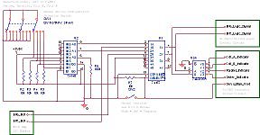
Hardware
Interface Development
After considering multiple design solutions, a hardware
interface system was designed to both condition input
signals to the DAQ and amplify output signals to hardware.
Most signal conditioning occurs in the Servovalve Test
Interface (STI) while the solenoid valves are controlled
by the Solenoid Valve Driver (SVD). Pressure transducers
are driven by external hardware provided by Boeing,
and the servovalve voltage controlled current source
is also external, but connects directly to the Servovalve
Test Interface. The signals processed by the hardware
interface are shown in the signal flow diagram in Figure
20.
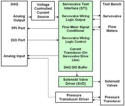
Figure
20. Servovalve hardware interface signal flow
diagram
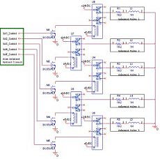
The components designed primarily by
ME5.3 are the Servovalve Test Interface and the Solenoid
Valve Driver (in green). Multiple subsystems are present
in the Servovalve Test Interface and the Solenoid Valve
Driver as they accomplish a variety of signal processing
tasks. The main components in the circuitry are shown
below in Figure 21. Each component is examined in detail
in the following section.
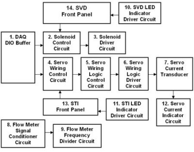
Figure
21. Circuitry
components in STI and SVD
| 1.
DAQ DIO Buffer
This circuit component shown in Figure 22 is
designed to isolate the DAQ DIO ports from the
interface hardware. All channels are digitally
isolated with 4N29 optoisolators. All inputs are
0-5 V logic signals from the DAQ breakout box.
The optoisolators are able to source up to 10
mA of current to the rest of hardware interface
circuitry.
2.
Solenoid Control Circuit
The solenoid control circuit shown in Figure
23 selects between a computer signal from the
DIO buffer circuit and a manually created signal
on the Solenoid Valve Driver front panel to send
to the solenoid driver circuit. |
 Figure
22. DAQ DIO buffer circuit schematic
Figure
22. DAQ DIO buffer circuit schematic |
| The circuit either reads bits
1 through 5 from the DIO Buffer or monitors the
position of five SPST switches on the front panel
of the Solenoid Valve Driver.Depending on the
position of the manual override switch on the
front panel, the circuit selects between a manual
signal or computer signal to send to the solenoid
driver circuit. |
|
Figure
23. Solenoid control circuit schematic |
Data selection is
implemented using two 74157 IC’s. The IC’s
can accept up to two sets of four inputs and select
a single set of four based on the logic state
of the SELECTAB input. Outputs of this circuit
go to the solenoid driver circuit to control the
state of the five solenoid valves on the test
bench and to the Solenoid Valve Driver LED indicator
driver circuit for display of solenoid and manual
override states. |
|
3.
Solenoid Driver Circuit
The solenoid driver circuit shown
in Figure 28 reads the selected control bits for
the solenoids from the solenoid control circuit
and uses five relays to control the state of each
solenoid. The control bits for the solenoids cannot
provide sufficient current to activate the relays,
so a BS170 n-channel enhancement mode MOSFET is
used to drive each relay. The relays are encased
in small PCB mount packages and are activated
with a 5 V 40 mA signal. Each is capable of driving
up to 2 A of DC current. Power for the solenoid
valves is provided by an independent 24 VDC power
supply that can source up to 10A of current. Each
solenoid valve requires 1.25 A of current to open,
which requires the solenoid power supply to be
able to source at least 6.25 A.
|
Figure
24. Solenoid driver circuit schematic
|
4.
Servovalve Wiring Control Circuit
Wiring configuration, shown in Figure 25, can be controlled
by either a two bit signal from the DAQ DIO buffer circuit
or manually by a rotary selector switch on the Servovalve
Test Interface front panel. As with the solenoid control
circuit, a SPST switch on the front panel controls the
SELECTAB input of a 74157 data selector IC. Depending
on the state of the switch, either the manual or computer
control signal is selected. To conserve outputs on the
DAQ DIO port, only two bits are used to control servovalve
wiring configuration. The rotary selector switch on
the front panel effectively creates a four bit signal
with the two bits worth of information. For data selection
to occur the signal must be encoded into a two bit signal.
| 
Figure
25. Servovalve wiring control circuit
schematic |
Encoding is accomplished using a 74148 priority
encoder IC. This IC can encode up to eight inputs
into a three bit signal. As only two bits are
needed, four of the inputs are tied high and
the most significant bit of the output is ignored.
The output is thus a two bit signal with the
same form as the signal from the DIO buffer.
|
After data selection, the two bit signal is passed
to the servo logic control circuit. Also, through the
use of a 74LS139 IC, the signal sent to the logic control
circuitry is decoded and sent to the Servovalve Test
Interface LED indicator driver circuit. This allows
the state of the wiring configuration to be indicated
on the front panel. The state of the manual override
switch is also sent to the LED driver circuit so that
its state is shown on the front panel.
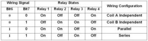
5.
Servovalve Wiring Logic Control Circuit
Servovalve wiring logic control diagram is shown in
Figure 26. Each servovalve has two coils that are used
to drive the torque motor. As there are two independent
coils, there are four possible different wiring configurations:
Coil A independent, Coil B independent, Coil A and Coil
B in parallel, and Coil A and Coil B in series. Each
configuration is used in practice for different control
situations. The user can control the wiring configuration
with a two bit signal sent from the DAQ DIO port or
with a manual signal from a selector switch on the front
panel. The table below summarizes the wiring states
associated with the bit states.
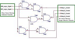 Figure
26. Servovalve wiring logic control
Figure
26. Servovalve wiring logic control
circuit schematic |
Table.
Servovalve wiring states/bit states
|
Control of the wiring states is implemented through
the use of a digital logic circuit consisting entirely
of NAND gates. The gates in use are of the 7400 series
TTL logic family. If part replacement or board replication
is ever necessary, the components in this circuit are
intentionally chosen to be easy to find and replace
at a low cost. The NAND gates receive the two bit signal
from the DIO port and decode the signal into control
signals for four relays.
Logic circuit design consisted of creating an individual
Karnaugh map to define the states of each relay control
signal as a function of the input bits. The result was
a sum of products form logic equation for each relay
state. The sum of products form is easily transferable
into purely NAND states, and after simplification the
resulting logic circuit is shown in the schematic above.
The timing diagram, shown in Figure 27, summarizes
the output of the logic circuit. Note that the relays
are on when the timing diagram is at 0 V and off when
the diagram is at 5 V. Comparison of the relay states
with the desired states in the logic table above shows
that the circuit functions as desired. Hardware testing
provides the same result. Also note that during transitions
some voltage spikes are present. These spikes are not
an issue because the response time of the relays is
far slower than the transition time of the logic signal
from the DIO port. Also, all tests are conducted with
a single, preset wiring configuration. Transitions do
not occur during tests so there is no possibility of
adverse effects from transition timing.
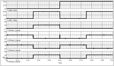
Figure 27. Wiring logic timing diagram
6.
Servovalve Wiring Logic Driver Circuit
Wiring state is controlled by four relays as
shown in Figure 28. The 7400 series chips in
the servo wiring control circuit cannot provide
enough current to drive the relays directly,
so an intermediate amplifier is in use. BS170
n-channel enhancement mode MOSFET’s are
used to amplify the logic signal. No special
power requirements are necessary as all components
are driven by a common 5 V power supply. The
current signal for the servovalve coils is provided
by an external current source in the Boeing
Servo Controller II.
|
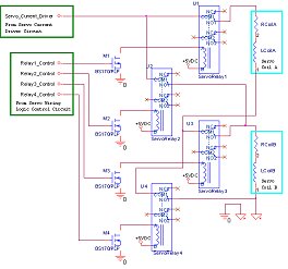
Figure 28. Servovalve wiring
logic driver circuit schematic
|
| 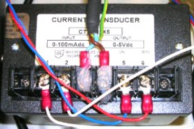
Figure 29. Servovalve current
transducer
|
7.
Servo Current Transducer
The servo current transducer shown in Figure
29 is an off-the-shelf device that provides
a 0-5 V analog voltage signal that is linearly
proportional to the electrical current that
flows through it. It is placed in series with
the servovalve coils to monitor servovalve current.
|
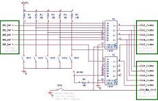
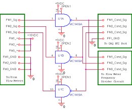
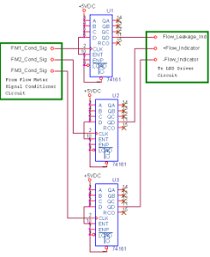
| 8.
Flow Meter Signal Conditioner
Flow meter signal conditioning,
shown in Figure 30, is implemented through the
use of an MC1489A line driver IC’s. This
IC can receive input signals that range from -30
V to +30 V and converts the signal to a TTL level
logic signal. The conversion point can be programmed
with a resistor placed from the supply voltage
to pin number two. The default transition point
(no external resistor) is approximately 2.5 V.
The three flow meters on the test bench output
a 0-10 V pulse train, so the default transition
point is adequate. Output signals are sent to
the DAQ PFI port where counters are used to measure
the frequency of the pulse train and thereby measure
flow rate. Outputs are also sent to a frequency
divider circuit for front panel display purposes. |
Figure
30. Flow meter signal conditioner
circuit schematic
|
|
Figure
31. Flow meter frequency divider
circuit schematic
|
9.
Flow Meter Frequency Divider Circuit
Three LED’s on the front
panel of the Servovalve Test Interface are used
to provide a visual indication of flow in the
test bench. The LED’s flash when the flow
meters are measuring a flow. The drive signal
for the LED’s is derived from the pulse
train output of the flow meters. Unfortunately,
the frequency of the flow meters at high flow
rates is 600-800 Hz, which is far too fast for
the human eye to notice. As a solution to this
problem, the frequency of the pulse train is
divided by 16 using the 74161 four bit synchronous
binary counter IC. This makes the flash frequency
of the indicators at high flow rates around
40 Hz which is approximately the upper end of
the visual range. The circuit schematic is shown
in Figure 31.
|
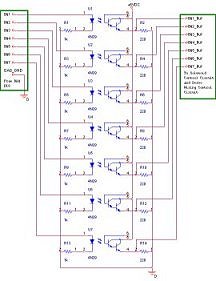
| 10.
Solenoid Valve Driver LED Indicator Driver Circuit
LED’s on the front panel of the Solenoid
Valve Driver are all driven by a single ULN2003A
Darlington array IC. This IC acts as an inverting
open-collector buffer for digital logic signals.
The IC is necessary because TTL IC’s used
in the interface circuitry are unable to provide
enough current to both drive indicators satisfactorily
while still driving other logic IC’s. As
an added advantage, the ULN2003A has a common
diode protected lamp test line. When this line
is brought to ground, all LED’s connected
to the IC will light so the user can see if any
lamps are not functioning properly. The lamp test
button can be found on the front panel. A schematic
of that system is shown in Figure 32. |
Figure
32. Solenoid Valve Driver LED
indicator driver circuit schematic
|
The manual override signal that is input to this circuit
is low when the manual override function is activated.
LED’s are turned on by the ULN2003A with a high
signal on the input line, thus for a manual override
indicator to function correctly on the front panel,
the signal must be inverted prior to reaching the LED
driver IC. This is accomplished with an inverter in
a 7404 IC as shown).
11.
Servovalve Test Interface LED Indicator Driver Circuit
LED’s on the Servovalve Test interface are driven
in the same way as on the Solenoid Valve Driver, as
shown in Figure 33. The ULN2003A IC’s provide
a common collector output with lamp test function to
drive all digital indicators. Similarly to the manual
override signal for the Solenoid Valve Driver, the manual
override signal for the servovalve wiring configuration
and the wiring state indicators are all active low signals.
The inputs are inverted prior to reaching the LED driver
with five inverters in a 7404 inverter IC. All other
signals are active high and are sent directly to the
inputs of the LED driver IC.
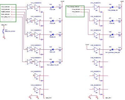
Figure 33. Servovalve
Test Interface LED indicator driver circuit
12.
Servovalve Current Indicator Circuit
The user of the Servovalve Test Interface is provided
with two LED’s on the front panel that indicate
the magnitude and direction of current flow in the servovalve,
as shown in Figure 32. The circuit schematic is shown
in Figure 34. One LED is used to indicate positive current
flow and the other indicates negative. The brightness
of the LED’s corresponds to the amount of current
flowing in the servovalve. The LED’s are designed
to reach maximum brightness when 20mA of current is
flowing through the servovalve, which is reasonable
for nearly all servovalve tests. The four op amps in
an LM348 IC are used to create this circuit. The first
op amp, U1A, buffers the current signal so that the
LED indicator circuit will not interfere with the current
signal sent to the analog input of the DAQ. U1B is an
inverting amplifier calibrated such that the supply
voltage will appear at the amplifier’s output
when 20mA of current are flowing through the servovalve.
U1C and U1D provide DC offsets for the two indicator
LED’s so that their response is more linear. The
LED’s used require about 1.7V of forward voltage
before they will light, so the two DC offset amplifiers
are designed to provide almost that much offset (approximately
1.6V). Note that these LED’s will not respond
to the lamp test function because they are controlled
by an analog signal. Their signal cannot be sent through
the ULN2003A IC’s because it is a digital line
driver, not analog.
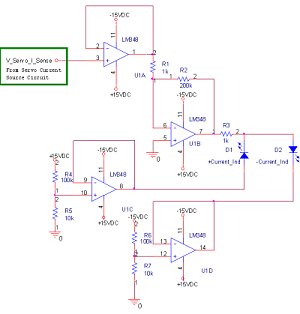
Figure 34. Servovalve current indicator circuit
schematic
13.
Servovalve Test Interface Front Panel
The front panel layout of the Servovalve Test Interface
and Solenoid Valve Driver can be seen in Figure 35.
All functions are described in detail with the accompanying
schematic diagram in the previous section.
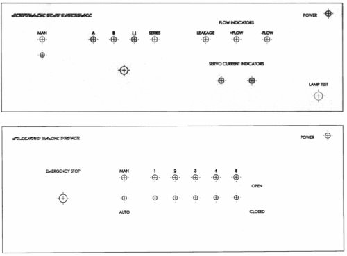
Figure 35. (Top) Servovalve Test Interface
Front Panel
(Bottom) Solenoid Valve Driver Front Panel
Next Page -
Pictures and Endnote
|